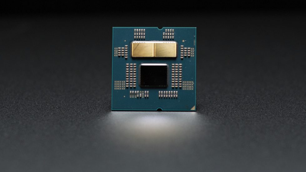
AMD's Ryzen 7000 launch is bigger than just the processors. The processor architecture is changing, but it's also being accompanied by changes to everything from the chipset to the physical socket that the chips plug into. The last time this many things changed at once was back in 2017, when the first-generation Ryzen chips originally launched.
So we're publishing two Ryzen pieces today. One is a look at the actual chips' performance and power efficiency, located here. This one will focus on all the other changes, including the ones that will be with us long after Ryzen 7000 is old news.
We'll split this piece up into four parts that cover the four major components of the Ryzen 7000 launch: 1) the Zen 4 CPU core, 2) the on-chip I/O die that supports the CPU's non-CPU features and handles internal connectivity, 3) the 600-series chipsets that handle most external connectivity, and 4) the physical AM5 socket that will outlive all of the other components by a few years.
Table of Contents
- Zen 4 CPU, in brief
- The I/O die
- Selecting an optimal RAM speed
- The integrated GPU: Two RDNA GPU cores, mostly USB-C outputs
- Built-in USB flashback support
- Socket AM5: More power, support through 2025
- Four chipsets are actually two chipsets (that are actually one chipset)
- EXPO memory overclocking profiles
Zen 4 CPU, in brief
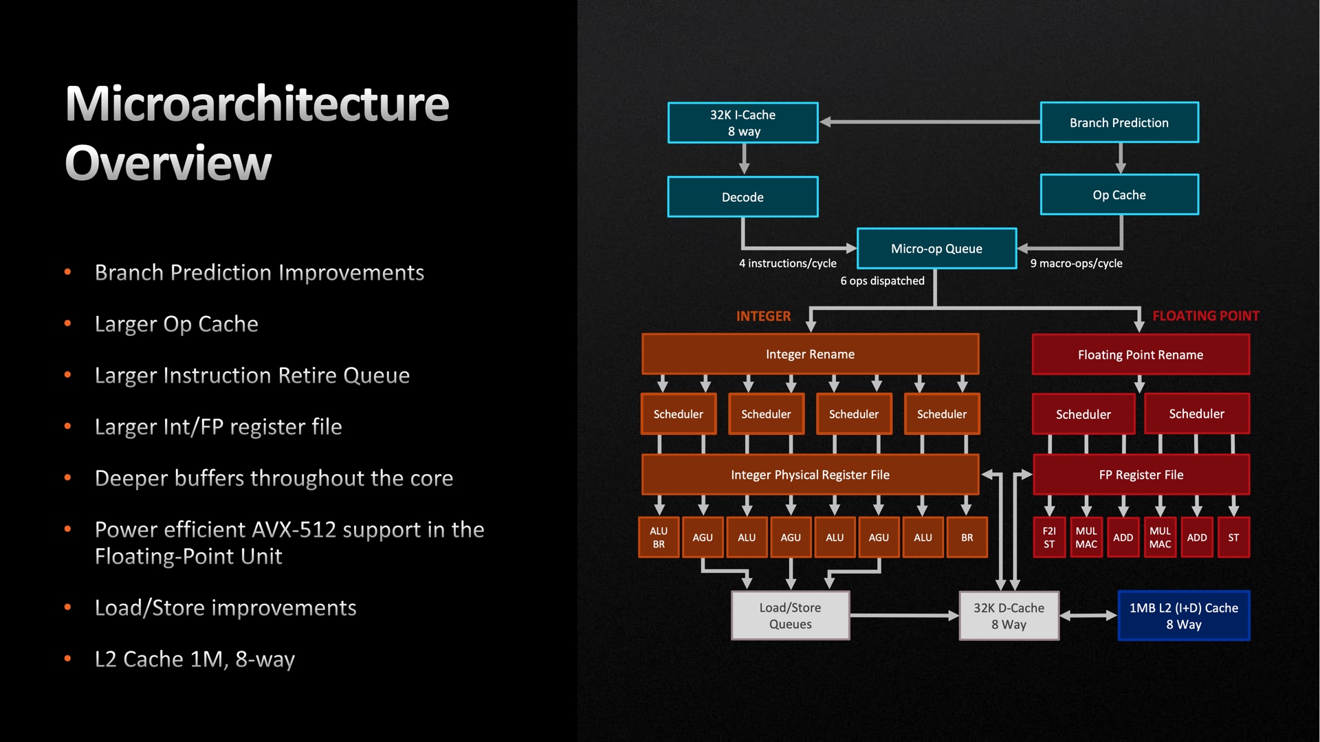 The high-level Zen 4 architectural overview. Zen 4 is a revision of Zen 3, where AMD called Zen 3 a "ground-up" redesign.AMD
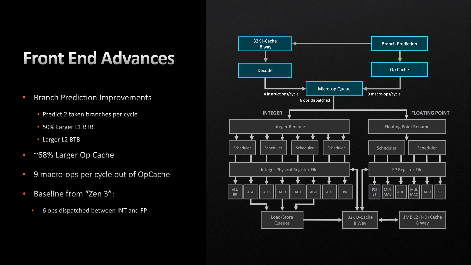 Most of the performance gains come from front-end improvements that keep the processor fed.AMD
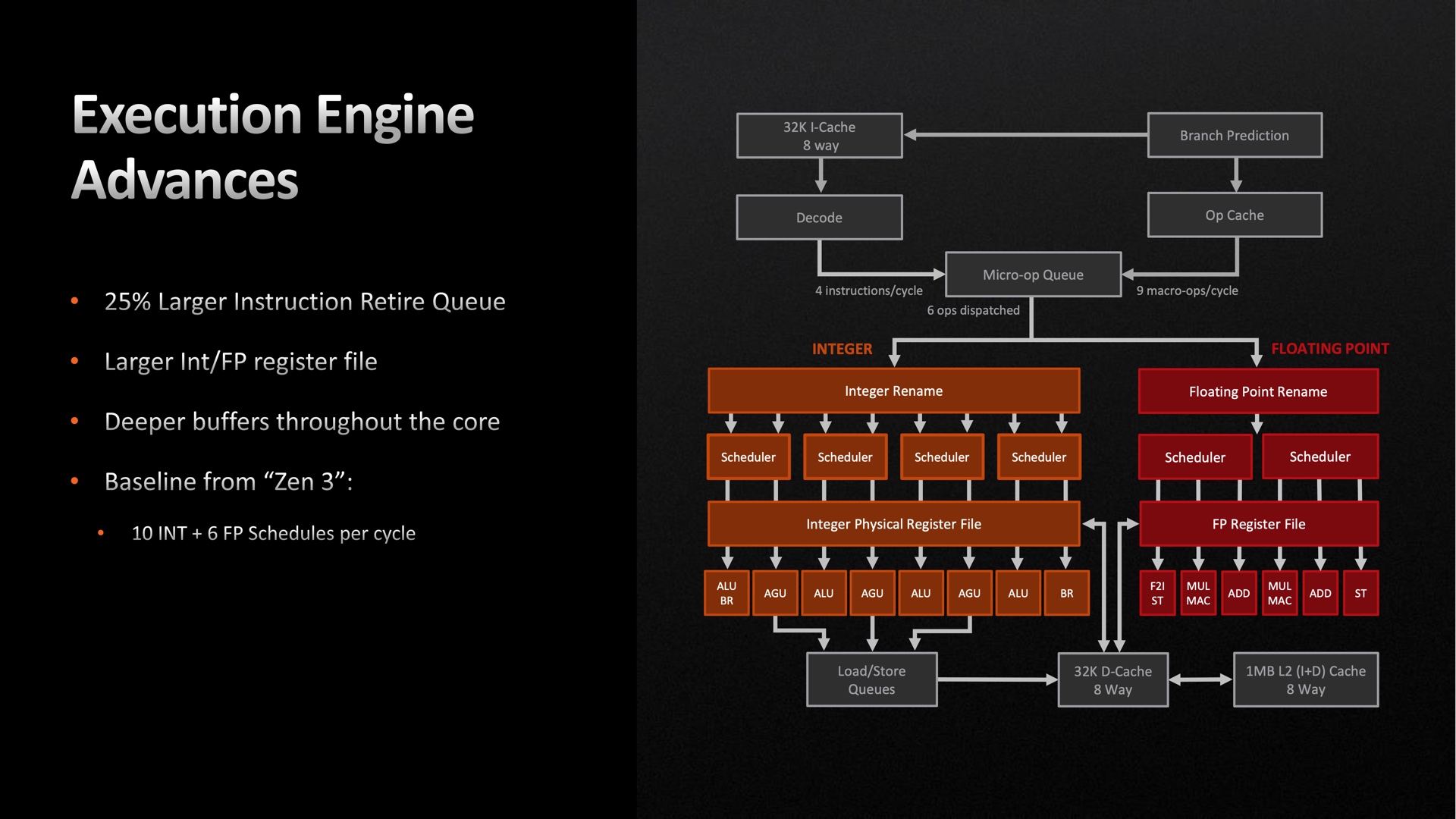 Though there have been some execution improvements as well.AMD
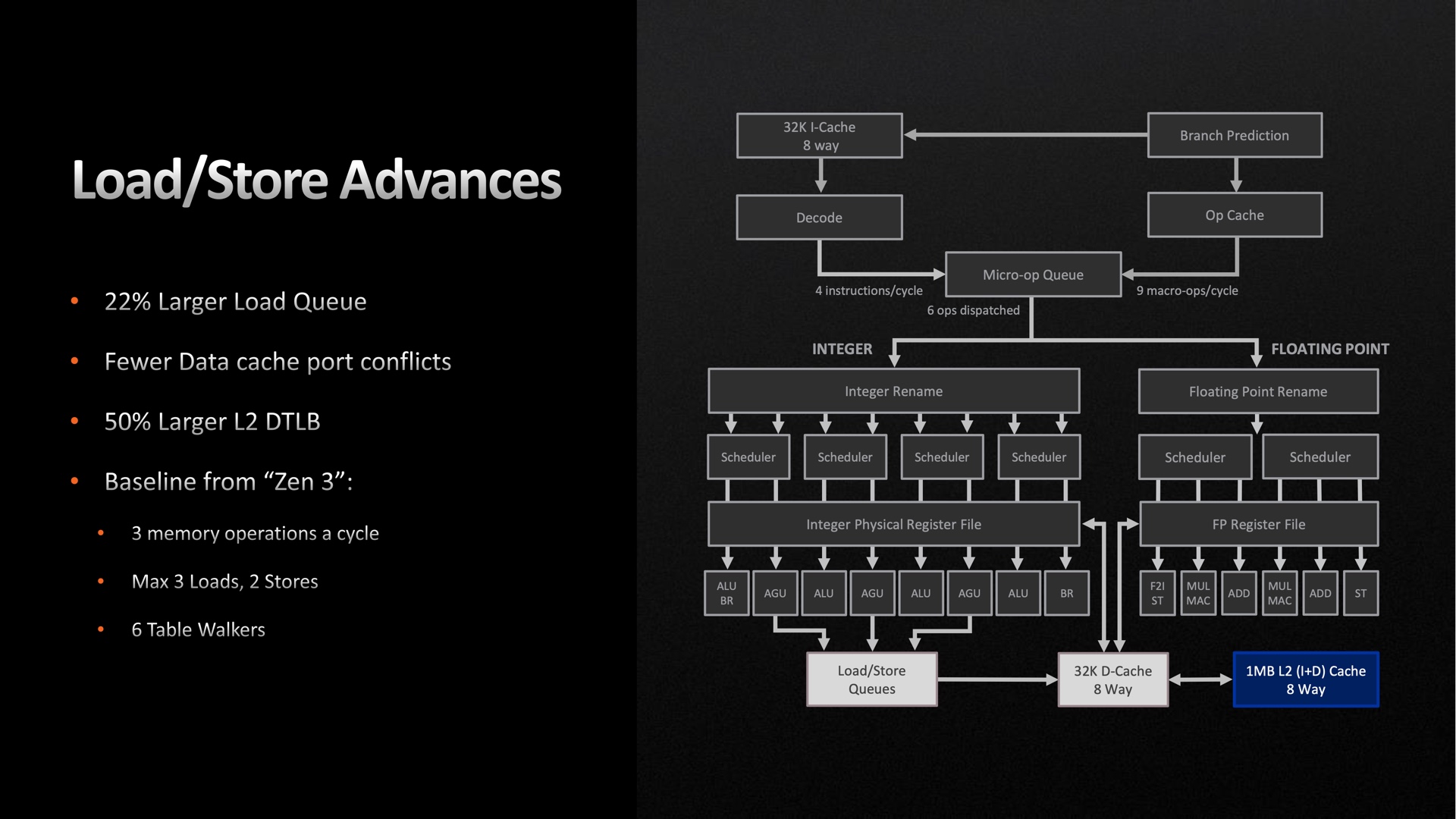 AMD has increased the size of the load queue and bumped up some cache sizes.AMD
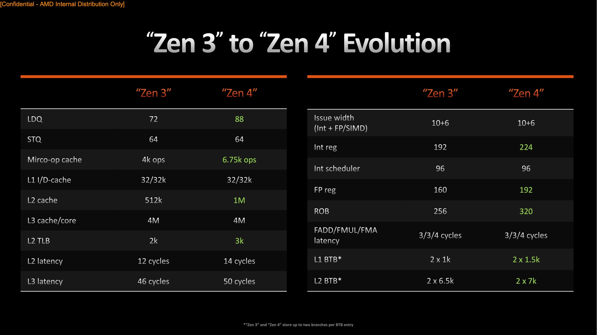 A side-by-side comparison of Zen 3 and 4.AMD
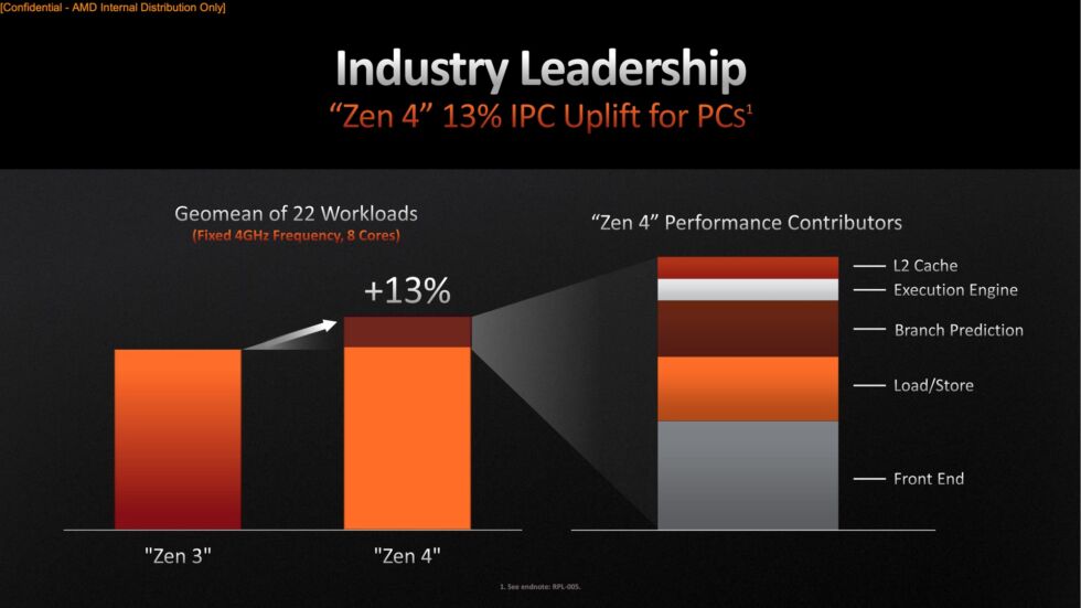
AMD promises roughly 29 percent faster single-core CPU performance in Zen 4 relative to Zen 3, which the tests in our review more or less back up. A little under half of this increase comes from architectural improvements that boost Zen 4's instructions-per-clock (IPC) count, while the rest comes from clock speed boosts. Clocks for Ryzen 5000 processors all peaked just short of 5 GHz, while Ryzen 7000's CPUs all boast peak clock speeds well above 5 GHz.
On the architecture front, AMD says that Zen 4 is a refinement of Zen 3 rather than a ground-up redesign. Many of the building blocks of Zen 3 are still present: eight-core Core Complex Dies (CCDs) made from one eight-core Core Complex (CCX), which shares a large 32MB cache among all eight CPU cores (or six, in the 7600X and 7900X). Ryzen CPUs consist of either one or two CCDs and an I/O die (IOD), linked with AMD's Infinity Fabric interconnect.
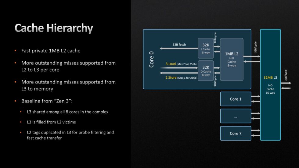
The bulk of Zen 4's IPC improvements come from an improved front-end design, with a faster branch predictor that can predict two branches per clock cycle instead of one, as well as larger L1 and L2 Branch Target Buffer caches and Op Cache. Zen 4 also features improvements to the load/store unit, which has a 22 percent larger load queue and a larger L2 cache. Each individual CPU core inside the CCX also has its own 1MB chunk of memory—twice as much L2 as each Zen 3 core.
To make these additions and improvements without increasing power usage, Zen 4 CCDs are manufactured on a 5 nm process from TSMC, an upgrade from the 7 nm process used for both Zen 2 and Zen 3. This enables Zen 4 CCDs to use nearly 57 percent more transistors than Zen 3 CCDs (from 4.15 billion to 6.5 billion) while making die sizes smaller overall (70 mm squared, down from 80.7 mm; it's also smaller than the 74 mm squared Zen 2 CCD die).
Because the CCX and CCD core counts are the same as in Zen 3, this means that core counts stay level for another generation—you can get as many as 16 cores in the Ryzen 9 5950X CPU, spread across two fully enabled CCDs. Sketchy rumors suggest that Zen 5 might switch to using a hybrid architecture split between large performance cores and smaller efficiency cores, as both Apple and Intel have done, but for now, every core in a Zen 4 CCD is the same size and has the same performance and capabilities.
Aside from general performance improvements, Zen 4 also adds support for AVX-512 processor extensions, both the foundational AVX512F instructions and a handful of others. But rather than building a large 512-bit SIMD block as Intel did, Zen 4 will process AVX-512 instructions by running them through its 256-bit SIMD. This comes with trade-offs—Zen 4 will need two clock cycles to process AVX-512 instructions instead of one, but unlike Intel CPUs with AVX-512 support, AMD's design also won't use nearly as much power or generate as much heat, allowing it to keep the clock speed higher. (It doesn't take up as much die space, either.)
By AMD's admission, its AVX-512 implementation won't be as fast as Intel's, but it feels like AMD made the right trade-offs given the niche-ness of AVX-512 support in the first place. Despite creating and pushing the instructions, Intel's 12th- and 13th-generation CPUs officially don't support AVX-512 at all, so even a less-speedy implementation from AMD is better than what Intel is currently offering on the desktop.
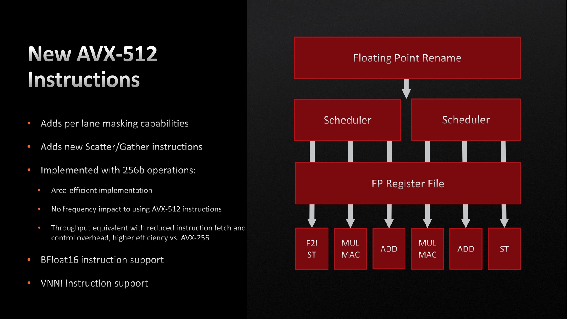 AMD's AVX-512 implementation uses a 256-bit wide SIMD, which means it needs two clock cycles to execute them but can run at higher clock speeds with lower power use and temperature than Intel's implementation; it also saves on die space.AMD
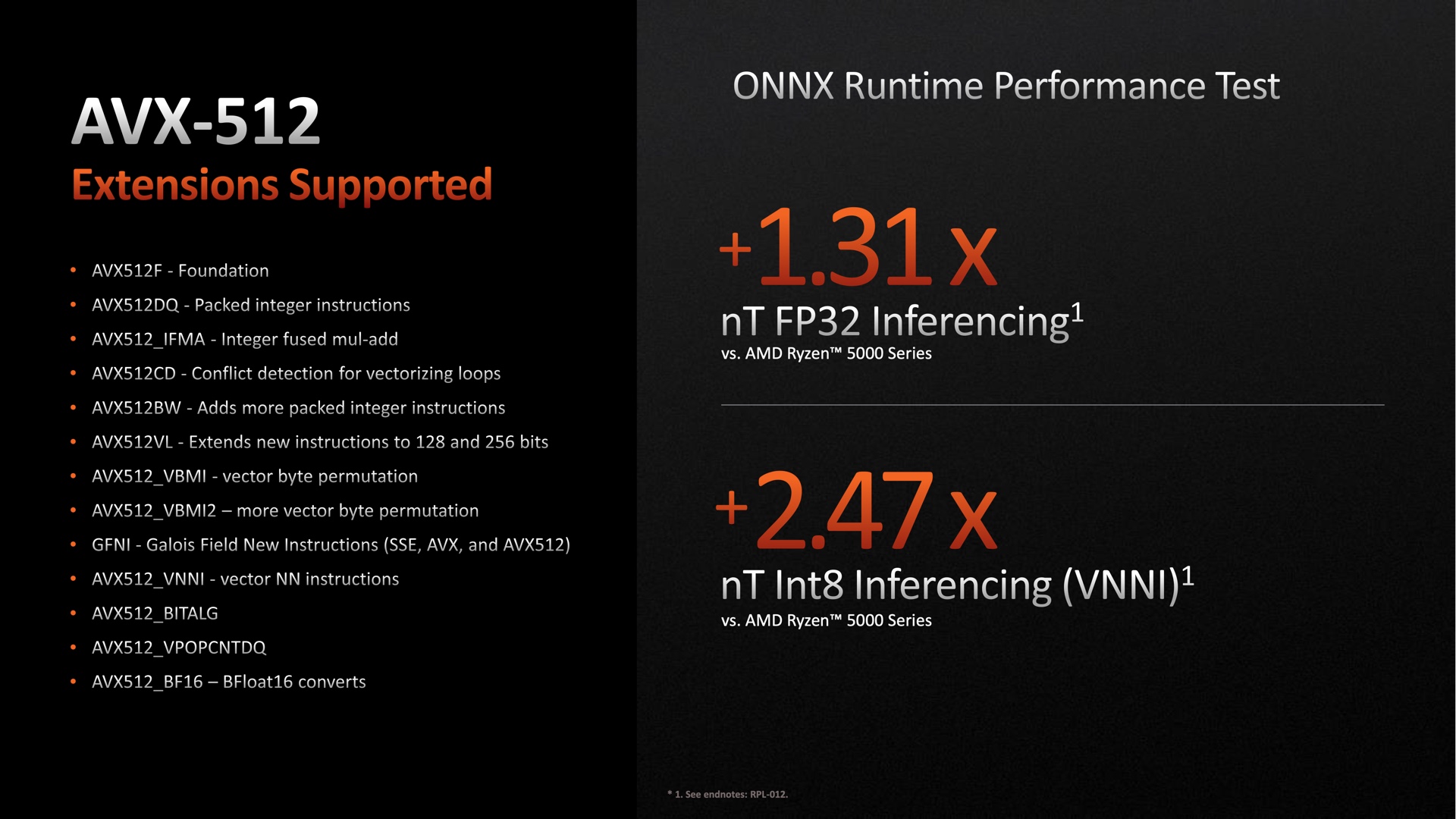 A list of the AVX-512 instructions supported by Zen 4.AMD
As for what's next for Zen 4, AMD's roadmap lists separate 3D V-Cache versions of Ryzen 7000, and we know that mobile processors are coming in the form of the "Phoenix" and "Dragon Range" chips. Less-expensive versions of the Ryzen 7000 CPUs will hopefully follow at some point as well—we had to wait almost a year and a half for $200-and-under Ryzen 5000 CPUs on the desktop, but hopefully the manufacturing and supply chain pressures that made that decision necessary have cleared up enough that we see cheaper Zen 4 chips a bit sooner.
The I/O die
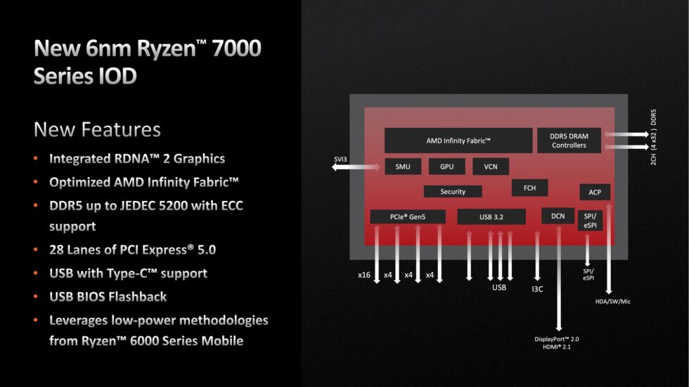
Zen 4 is an impressive jump from Zen 3, but if anything, the I/O die (IOD) is an even bigger departure from previous chips.
In AMD's processors, the IOD is a separate piece of silicon on the CPU package that has been manufactured on a more-mature, less-advanced process than the CPU dies. The benefits of scaling down these chipset functions aren't as noticeable or important as they are for the CPU cores themselves, so AMD keeps them physically separate, tied together via the Infinity Fabric interconnect. Both Zen 2 and Zen 3 desktop processors used the same 12 nm I/O die, which means it has been a couple of generations since we've seen major improvements here.
The Ryzen 7000 IOD has a new DDR5 memory controller with support for ECC RAM in motherboards that also support ECC RAM (but, unlike Intel, there's no DDR4 controller—it's DDR5 or bust). The processor can supply up to 28 lanes of PCIe 5.0 bandwidth, though motherboards with non-"Extreme" chipsets will still use PCIe 4.0 for the GPU slot. There's a new integrated GPU, a first for non-APU Ryzen processors. The IOD also includes its own USB controller with support for up to four 10Gbps USB 3.2 Gen 2, included partly to enable DisplayPort-over-USB-C connections to the integrated GPU and the built-in USB flashback functionality.
Selecting an optimal RAM speed
The DDR5 memory controller supports DDR5-5200, as far as officially sanctioned JEDEC memory standards go. But as with most motherboards these days, one-click RAM overclocking is both supported and encouraged. AMD recommends a "sweet spot" of DDR5-6000 to get the best performance out of Ryzen 7000.
Explaining why is a bit complex. In short, RAM speed (MCLK), memory controller speed (UCLK), and the speed of the Infinity Fabric interconnect (FCLK) are all tied together, part of the reason why Ryzen's performance has historically been more sensitive to memory bandwidth than Intel's.
In Ryzen 3000 and 5000 CPUs, the recommended strategy was usually to try to keep MCLK, UCLK, and FCLK running at the same speed (also called a 1:1:1 ratio). If you set your memory clock speed too high for the Infinity Fabric to keep up, the Infinity Fabric clock speed could actually fall back to a lower speed, introducing latency that could offset the performance benefit of the faster memory (and wasting whatever extra money you spent on super-fast RAM). For these CPUs, AMD typically recommended DDR4-3600 as a sweet spot, since the RAM, memory controller, and Infinity Fabric could all easily handle an 1800 MHz clock speed, and DDR4-3600 was generally a lot cheaper than faster RAM kits while being only slightly more expensive than slower RAM kits.
For Ryzen 7000, higher RAM speeds for DDR5 make a 1:1:1 ratio harder to achieve, so AMD recommends keeping the memory clock and memory controller clock (MCLK and UCLK) synced at 1:1 while the Infinity Fabric (FCLK) runs at a slightly elevated speed of 2,000 MHz (the default ranges between 1,600 and 1,800 MHz). For RAM speeds above DDR5-6000, AMD says the memory controller clock can no longer keep up, so it drops to a 2:1 ratio. Spend money on a (fictitious, currently) DDR5-8000 kit, and you'd end up with a memory clock of 4,000 MHz but a memory controller clock of just 2,000 MHz, rather than the controller clock of 3,000 MHz you get with DDR5-6000, reducing or erasing whatever performance benefits you wanted to achieve by using faster RAM.
The integrated GPU: Two RDNA GPU cores, mostly USB-C outputs
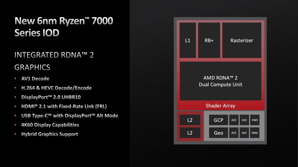
For the first time, all of AMD's CPUs include a basic integrated GPU. All four of the CPUs introduced today include a GPU with two compute units (CUs) built into the I/O die and based on the same RDNA2 architecture as the Radeon RX 6000 dedicated GPUs and the Ryzen 6000-series integrated GPUs.
These GPUs are primarily made with CPU-focused workstations and business desktops in mind, systems where graphics performance is non-critical but being able to drive a couple of monitors in a small power envelope is handy. For anyone who throws a dedicated GPU into their system, you can either ignore the integrated GPU altogether or keep it turned on so you can use its video encoding and decoding blocks or its display output capabilities. As with Intel's integrated GPUs, AMD's can operate in hybrid mode, using a dedicated GPU to render content that is then displayed on a monitor connected via the integrated GPU.
AMD emphasized over and over again that these aren't meant to be gaming GPUs, nor are they replacements for the G-series APUs that AMD releases. Those APUs typically contain somewhere between six and 12 GPU cores, still nowhere near what a dedicated GPU includes but substantially more than the Ryzen 7000 I/O die. In our review, we found that the new Ryzen GPU and Intel's current UHD 770 GPU perform pretty similarly. As a gaming GPU, 2D performance is fine, performance in older games is OK, and it's fine for Minecraft—but expect 720p and low settings in more modern titles.
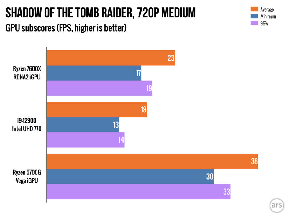
But these still are RDNA-based GPU cores, and they do confer benefits even for gaming systems with dedicated GPUs. The integrated GPUs will support a maximum of four separate display outputs, one over either HDMI or DisplayPort, plus another three over USB-C using HDMI 2.1 or DisplayPort alt modes. This is a nice change from the status quo, where desktop USB-C ports can frequently only handle data rather than doubling as display outputs as they do on most laptops. AMD says that the integrated GPU can drive up to three 60 Hz 4K displays at once, but it was noncommittal about higher-than-60 Hz output. In our testing, the GPU had no issue simultaneously driving one 4K display at 60 Hz over HDMI and one 4K display at 144 Hz via DisplayPort-over-USB-C, so they can clearly do a bit better than AMD says.
The new GPUs share other features in common with other RDNA2 GPUs, too. They support variable refresh rates via FreeSync. Their video encoding and decoding block supports decoding of AV1 (and VP9) video streams, but you'll still need an Intel Arc or Nvidia RTX 4000-series GPU to support hardware-accelerated encoding of AV1; the encoding block does support 8- and 10-bit H.265 and H.264 video. They can even do hardware-accelerated ray tracing, though they're so slow that there is no practical benefit to it.
Built-in USB flashback support
One other handy, common-sense addition to the I/O die is built-in USB flashback support—the ability to flash your BIOS to a newer version even if the current version doesn't support the CPU you have installed. Not having this feature could have been a huge headache when new AM4 processors launched; if you wanted to buy a modern CPU with a slightly older motherboard to save some money, you could never assume that the motherboard would actually ship with a BIOS that supported that CPU, even if the motherboard maker had released an updated BIOS already.
AMD's only official solution for this problem on AM4 motherboards was kludgy and involved making a warranty claim against your new processor to request an old low-end CPU loaner as a "boot kit." Midrange-to-high-end motherboards ended up implementing CPU-less BIOS flashing via USB to get around this, but this is the first time AMD has implemented it into the platform directly.
AMD tells us it expects some manufacturers to stick with their own USB flashback implementations, and it isn't requiring motherboards to actually enable the built-in version either; motherboard makers will need to implement some kind of physical switch or jumper to enable the feature, and AMD isn't making anyone do it. We may still see some budget-y motherboards ship with no version of USB flashback, AMD-enabled or otherwise. But the company hopes that having the capability built in will end up pushing most boards to include it.
Socket AM5: More power, support through 2025
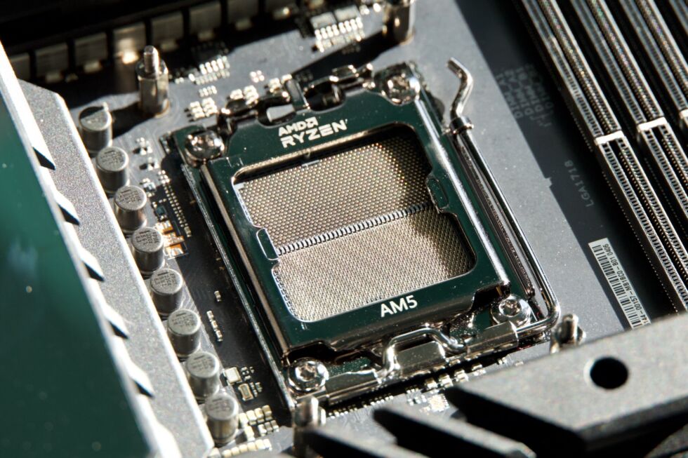
Chipsets and processors will change, but Ryzen 7000 ushers in the successor to 2017's AM4 processor socket. Socket AM5 is a 1718-pin land-grid array (LGA) socket, meaning that its pins are on the motherboard instead of on the CPU. One thing the additional pins allow for is more power delivery—from a rated maximum of 142 W for AM4 to a maximum of 242 W for AM5. This also lets AMD increase the TDP ratings of newer Ryzen CPUs, from 105 W to 170 W.
These power ceilings are far above what you need to get good performance out of Zen 4; the Ryzen 7950X in our review performed well even when set to a 105 W or 65 W TDP instead of its normal 170 W, and the 7600X performed nearly identically set to 65 W or its default 105 W. But if AMD intends this socket to last until at least 2025, it will probably see Ryzen 8000 or Ryzen 9000 processors someday, too; if AMD wants to increase performance without the benefit of a new manufacturing process, or if it wants to increase the maximum number of CPU cores from 16 to something higher, or if 3D V-Cache chips continue to run hotter and more power-hungry than their V-Cache-less counterparts, AM5 gives AMD a good amount of future headroom.
Unlike Intel's LGA 1700 socket, AMD has been able to keep the dimensions of its CPU packages the same in the move from AM4 to AM5, which means that very nearly all existing CPU coolers with AM4 mounting hardware should be able to mount to AM5 processors and motherboards. Both a cheapo Vetroo V5 air cooler and a Corsair iCue H115i AIO pump worked just fine with the AM5 CPUs in our testing.
AMD has committed to support socket AM5 through at least 2025, which implies it will probably see at least two major Ryzen CPU refreshes (plus a bunch of minor releases in between). Three years sounds relatively paltry compared to AM4, which had a solid five years of support, but AMD only promised to support AM4 through 2020 back when it launched in 2017. There's precedent for underpromising and overdelivering on the CPU support front.
Four chipsets are actually two chipsets (that are actually one chipset)
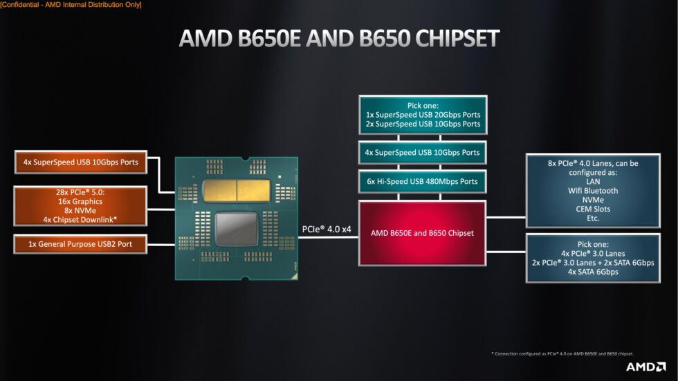
All system I/O that the processor's built-in I/O die doesn't handle is still handled by the chipset, an external die that is connected to the CPU over the PCI Express bus. AMD has only made a single physical chip for this generation, which is offered in a total of four configurations.
Let's start with the lower-end chipset since it's the basic building block AMD is working from. The B650 chipset is connected to the CPU via four PCIe 4.0 lanes. It can enable as many as 12 extra USB ports beyond what the IOD supports, plus eight general-purpose PCIe 4.0 lanes that can be used to support additional M.2 slots, Wi-Fi modules, LAN ports, or other internal accessories. And another four PCIe 3.0 lanes can be used to support another NVMe slot, 6Gbps SATA ports, or some combination of both.
Eight of the Ryzen CPU's 24 PCIe 5.0 lanes are used to support PCIe 5.0 SSDs, while 16 more run to the main PCIe slot you use for GPUs. In a standard B650 motherboard, the GPU slot will only run at PCIe 4.0 speeds. The next chipset, B650E, is identical to B650, but motherboard manufacturers will ensure that the system's main PCI Express x16 slot can also handle PCIe 5.0's increased signaling requirements. This is the only difference between B650 and B650E.
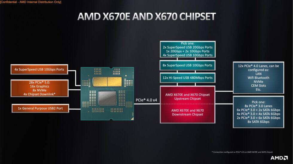
The X670 chipset uses the exact same die as the B650—there are just two of them, one referred to as the "upstream chipset" and the other designated the "downstream chipset." Everything about an X670 board's I/O is exactly doubled compared to B650, except you only get 12 general-purpose PCIe 4.0 lanes where you'd expect to get 16. That's because four of the chipset's PCIe 4.0 lanes are used to connect the upstream and downstream chipsets, in addition to the four used to connect the chipsets to the CPU.
As with the B650E, X670E boards are identical to X670 boards, but they support PCIe 5.0 speeds for the GPU slot rather than PCIe 4.0.
AMD reiterated to us that all four of these chipsets will be capable of overclocking, as they always have been—there's no artificial gating of overclocking to higher-end chipsets and boards. But the X670 chipsets are still more likely to be included in boards with more robust power delivery and better voltage regulator modules—things you'll want if maximizing an overclock is really important to you.
EXPO memory overclocking profiles
Automated memory overclocking has become a popular way to wring out slightly higher performance from desktop systems in the last few years, especially for AMD systems where increased RAM speed can also increase the speed of the Infinity Fabric interconnect that allows the different CPU dies and the I/O die to communicate.
The main standard that most memory manufacturers and motherboard makers unified on is Intel's Extreme Memory Profile spec—RAM makers ensure that their sticks will run at standard DDR4 or DDR5 speeds out of the box, but XMP sticks also have faster speeds and tighter timings programmed into them. Users can head into their BIOS and load up these profiles with one click, "overclocking" their memory without having to worry about crashes or instability (at least, in theory).
With Ryzen 7000, AMD is introducing its own memory profiles, dubbed Extended Profiles for Overclocking (or EXPO). Rather than piggybacking off of XMP, AMD says that EXPO-certified RAM has been tested specifically with AMD's processors, allowing manufacturers to make additional speed and timing tweaks if they find that some settings work better with AMD's processors than Intel's. For users, the end result—one-click memory overclocking via the BIOS—is the same.
Ryzen 7000 CPUs and AM5 motherboards will be able to use regular XMP profiles, too. There's nothing blocking RAM makers from supporting both XMP and EXPO profiles in the same kit, but it's equally likely that Intel motherboards will just pick up support for EXPO profiles as well as XMP. Gigabyte and MSI have already announced that their Z690 and B660 motherboards will add EXPO support, and we suspect that other manufacturers will get on board. For now, be careful about trying to use an EXPO kit in an Intel board—the G.Skill Trident Z5 Neo EXPO RAM kit that AMD sent with our Ryzen review hardware did show us an XMP profile in the Gigabyte Z690 board we tested with, but the system wouldn't actually boot until I had dropped the RAM speed from DDR5-6000 down to DDR5-5800 (it ran fine at its rated speed on our AM5 system).
https://ift.tt/deR1CcJ
Technology
No comments:
Post a Comment